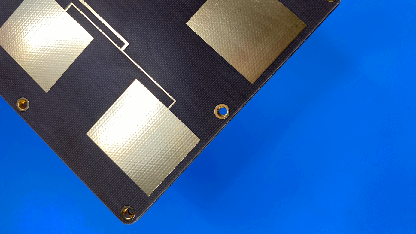
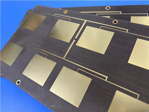
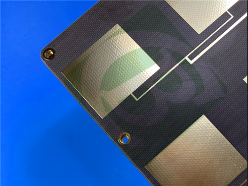
TLX-0 2-Layer 20mil Immersion Gold PCB for RF Microwave Applications
1. Introduction
TLX series laminates are made using PTFE fiberglass composites, offering reliability in a wide range of RF applications. This material is versatile due to its 2.45 - 2.65 DK range and available thicknesses and copper cladding. It is suitable for low layer count microwave designs.
TLX is a workhorse in the RF microwave substrate world where the fiberglass offers mechanical reinforcement wherever a substrate experiences severe environments such as:
Resistance to creep for PCBs bolted to a housing that encounters high levels of vibration during space launch
High temperature exposure in engine modules
Radiation resistance in space (see NASA's website for low outgassing materials)
Resistance to extreme environments at sea for warship antennas
Resistance to a wide temperature range for altimeter substrates during flight
TLX-0 is one the series materials with dielectric constant of 2.45 with tight tolerance of ±0.04.
2. Key Features
Low Dielectric Constant: 2.45 ±0.04 at 10GHz
Excellent Signal Integrity: Dissipation Factor of 0.0021 at 10GHz
Environmental Resistance: Low moisture absorption of 0.02%
Dimensional Stability: X axis CTE of 21 ppm/°C, Y CTE of 23 ppm/°C, Z CTE of 215 ppm/°C
Mechanical Durability: Strong Peel strength of 12 lbs/in
3. Benefits
Superior RF Performance: Excellent PIM Values in PCBs (measured at lower than -160 dBc)
Reliable Operation: Excellent Mechanical & Thermal Properties
Stable Electrical Characteristics: Low and Stable Dk, Tightly Controlled DK, Low DF
Environmental Durability: Dimensionally Stable, Low Moisture Absorption
Safety Certified: UL 94 V0 Rating
Design Flexibility: For Low Layer Count Microwave Designs
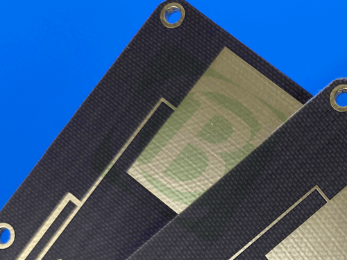
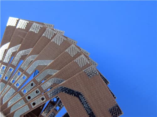
4. PCB Construction Details
| Parameter |
Specification |
| Base Material |
TLX-0 |
| Layer Count |
2-layer |
| Board Dimensions |
175mm × 90mm = 10PCS, ±0.15mm |
| Minimum Trace/Space |
5/7 mils |
| Minimum Hole Size |
0.3mm |
| Blind Vias |
No |
| Finished Board Thickness |
0.6mm |
| Finished Cu Weight |
1oz (1.4 mils) outer layers |
| Via Plating Thickness |
20 μm |
| Surface Finish |
Immersion Gold |
| Top Silkscreen |
No |
| Bottom Silkscreen |
No |
| Top Solder Mask |
No |
| Bottom Solder Mask |
No |
| Hole Treatment |
Hole plugged by solder mask ink (Green) |
| Electrical Test |
100% tested prior to shipment |
| Design Standard |
IPC-Class-2 |
| Artwork Format |
Gerber RS-274-X |
| Availability |
Worldwide |
5. PCB Stackup (2-Layer Rigid Structure)
Copper Layer 1 - 35 μm
TLX-0 Core - 0.508 mm (20mil)
Copper Layer 2 - 35 μm
6. PCB Statistics:
Components: 32
Total Pads: 73
Thru Hole Pads: 51
Top SMT Pads: 22
Bottom SMT Pads: 0
Vias: 105
Nets: 2
7. Typical Applications
Couplers, splitters, combiners, amplifiers, antennas and passive components
Radar systems, mobile communications
Microwave test equipment
Microwave transmission devices and RF components
8. Quality Assurance
Artwork Format: Gerber RS-274-X
Accepted Standard: IPC-Class-2
Availability: Worldwide
|
.png)
.png)